All In: US Places a Big Bet with October 17 Controls
US policymakers are wagering that industry and partners will align with US controls and that time and innovation are on Washington's side.
The United States is asserting its role as the de facto regulator of the global semiconductor industry in a new tranche of rules released October 17. The new package of rules appears designed to:
- Deter the world’s leading semiconductor firms from developing high-performance chips for the China market;
- Preempt circumvention by expanding the country scope for restrictions on advanced chips and semiconductor manufacturing equipment;
- Further constrain China’s ability to rely on older deep ultraviolet (DUV) immersion lithography equipment to produce advanced chips; and
- Slow down China’s cutting-edge AI chip design firms on national security grounds.
The 400-plus-page package of regulations takes care this time to lay out justifications for the controls and exemptions for US partners and certain “consumer-grade” chips. But the rules sustain the spirit of the original October 7, 2022 controls in their willingness to assert US extraterritoriality in novel ways, preempt technological advancements, and break new ground—for example, by inching toward regulating chips-as-a-service.
US policymakers are placing a big bet with these new rules. In designing the controls, the US is making an implicit assumption that industry and partner resistance will eventually give way to alignment with US regulations. The US is also wagering that time and innovation are on its side, even as China and others try to accelerate the substitution of US-origin technologies. Most of all, the US administration is assuming that tightening US-led tech controls on an economically insecure China amid an intensifying cycle of retribution can be managed with diplomatic guardrails.
Packed with punch
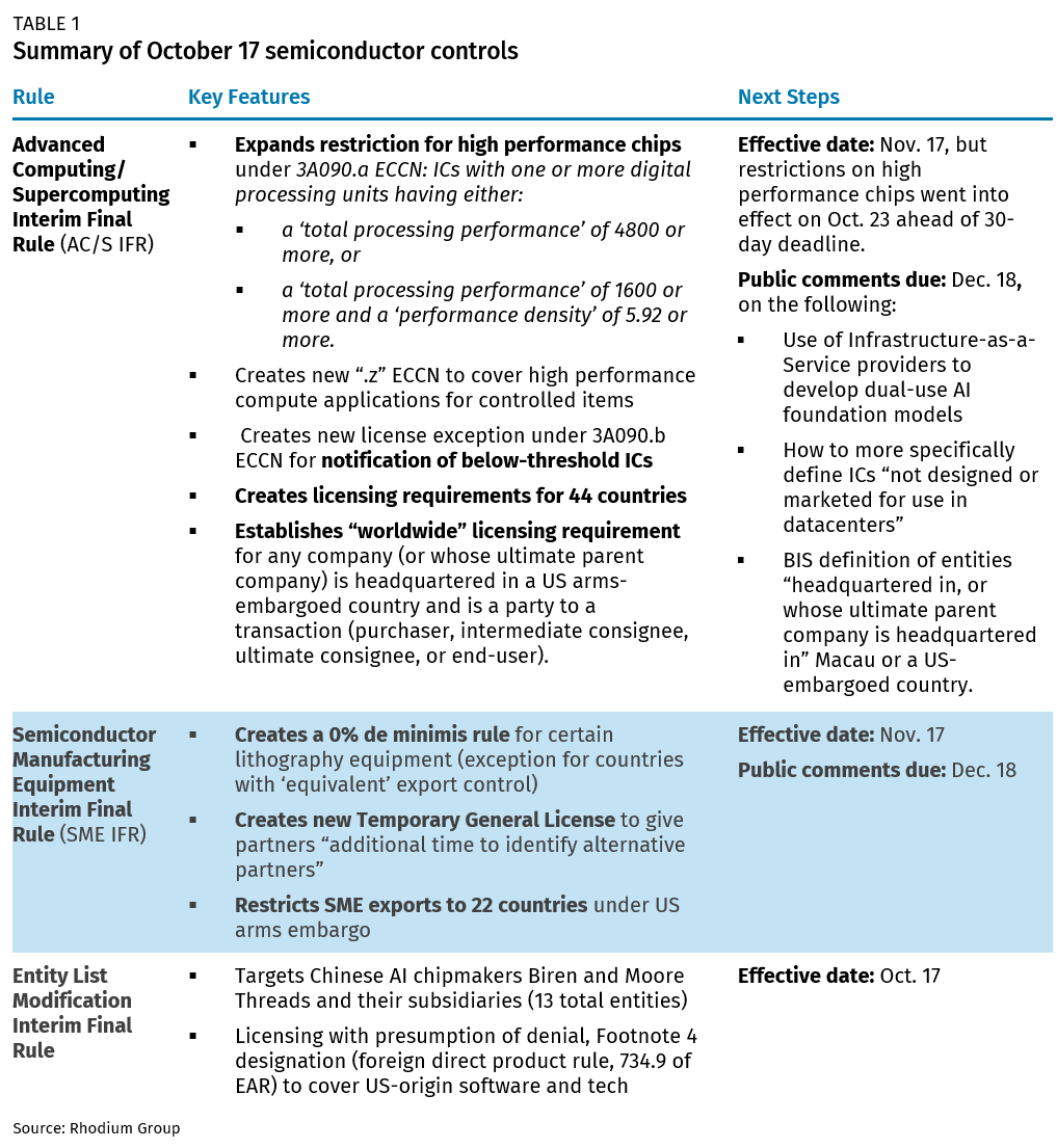
The October 17 package of export controls on AI chips, supercomputing, and semiconductor manufacturing equipment exceeds the ambition of the original October 7, 2022, semiconductor controls to constrain China’s ability to manufacture advanced chips and access high-performance computing power. As is typical with such dense regulations, tiny details buried in the text can carry a big punch.
Don’t even bother
The US is sending a clear signal to the world’s cutting-edge chip developers: don’t even bother putting time and resources into developing a high-performance computing chip for the China market. The rules will catch up.
Indeed, after watching Nvidia and Intel release cut-down versions of their deep-learning AI processors within months of the original October 7 controls, Nvidia’s A800 and H800 graphics processing units (GPUs) and Intel’s Gaudi2 system-on-chip (SoC) appear to now be banned for all Chinese entities and their subsidiaries. AMD had been debating developing a variant of its MI250 and MI300 GPUs for the China market, but those plans have now been short-circuited.
Agility is not typically a word used to describe a regulatory agency. In this case, however, the US Commerce Bureau of Industry and Security (BIS) recognized the imperfection of its original performance thresholds and iterated on them substantially within a year.
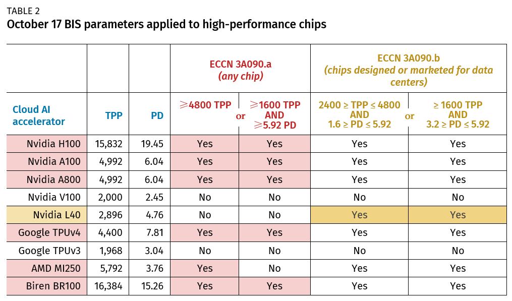
BIS focused on two key factors in setting the new parameters for high-performance compute chips under export control classification ECCN 3A090: (1) what is the raw compute power of the chip, and (2) what is the compute power in relation to its physical size?
In the new rules, BIS slightly tweaked the existing October 7, 2022 formula for determining raw compute power (now called “total processing performance,”1 or TPP). If 1) the TPP of an AI accelerator is at or above 4800 or 2) the TPP is at or above 1600 but the chip’s performance density (see below) is at or above 5.92, it can only be sold to China after acquiring an export license on presumption of denial.
With the newly introduced performance density parameter, BIS is examining the compute power relative to the size of the chip. The point is to discourage AI chip companies from combining multiple smaller chips to achieve comparable compute power. Performance density (PD) measures a chip’s compute power per square millimeter (TPP divided by the die area). In BIS’s own words, “a performance density parameter prevents the workaround of simply purchasing a larger number of smaller datacenter AI chips which, if combined, would be equally powerful as restricted chips.” BIS set the performance density threshold at 5.92, just slightly below the performance density of Nvidia’s A100 chip at 6.04 (see Table 1). As a result, if a chip’s TPP falls below 4800 but its performance density is above 5.92, the chip will be restricted under ECCN 3A090.a.
Notably, BIS has added another export control classification, ECCN 3A090.b, to control chips that fall just below the TPP and PD threshold. Chips that meet the 3A090.b requirements are in a grey zone: notification is required for export to China, Macao, and other destinations at higher risk of leaking controlled technology to China. Any high-end chipmaker trying to sell to China would have to calculate the risk of BIS updating the TPP and/or PD metrics after having some time to observe industry workarounds.
Notably, the October 17 rules focus on integrated circuits (ICs) that are “designed or marketed for use in data centers” to differentiate from “consumer-grade ICs” with AI capabilities that may be eligible for exemption. The theory of harm that BIS offers is that advanced computing chips that meet the new performance threshold and are used in data centers can be used to power AI frontier models with potential military applications, including unmanned intelligent combat systems, enhanced battlefield “situational awareness and decision-making,” and cyber warfare.
On these national security grounds, the US has not only tightened high-end chip access to China but has also directly targeted China’s premier AI chip designers: Biren and Moore Threads. These firms and their subsidiaries have been added to the BIS Entity List with a Footnote 4 Foreign Direct Product Rule designation, barring them from access to US-origin software and technologies. Even if Biren and Moore Threads (along with other Chinese AI chip designers who could land on the BIS Entity List for similar reasons) develop their own software stacks to compete with Nvidia’s powerful CUDA ecosystem, for example, they will still need leading-edge foreign fabs like TSMC to manufacture their chips. That supply chain node is now in jeopardy. US AI chip designers being told to keep out of the China market may at least take some solace in the fact that their biggest Chinese competitors are also getting pummeled by the new controls.
All eyes on SMIC (and ASML)
That is, unless China’s leading foundries SMIC and Hua Hong can advance their own manufacturing capabilities to produce indigenously designed advanced chips. But here again, the US has dealt a heavy blow in the updated rule for semiconductor manufacturing equipment.
In the new rules, the US instituted a 0% de minimis rule for certain lithography equipment but provides an exemption for exporting countries with equivalent export controls. Lithography, dominated by the Netherlands’ ASML, is the biggest semiconductor manufacturing equipment chokepoint in the value chain. In applying 0% de minimis, the US is effectively asserting jurisdiction over foreign-made lithography equipment regardless of whether there is an actual nexus to US content.
As we noted last month (see “Déjà Vu: Round Two of Chip Controls”), US regulators could exercise leverage over Cymer, a San Diego-based firm acquired by ASML in 2013 that produces excimer lasers for ASML’s lithography machines. Applying a 0% de minimis rule captures any shred of US technology or software linked to ASML, including those Cymer-made lasers, and even cases where no US product, service, technology, or person is involved.
Although the Netherlands begrudgingly joined the United States and Japan in issuing its own version of semiconductor export controls (the Dutch controls went into effect on September 1, with a grace period until January 1, 2024), the United States has apparently assessed that these controls did not go far enough. The ball is now back in The Hague’s court to “harmonize” their rules with those of the US.
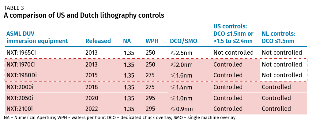
That is not the only detail causing heartburn for ASML and Dutch regulators, however. In the updated technical specs for lithography equipment in the US rules, BIS tweaked a key metric, called dedicated chuck overlay, or DCO. DCO accuracy (sometimes also called single machine overlay, or SMO) is a measure of how precisely a lithography machine can position the wafer during exposure.
A high DCO accuracy is critical to producing logic chips at or below 16/14nm and advanced memory chips using older lithography machinery. In a process called multi-patterning, the pattern is split into multiple parts, or sequences, to create structures on the wafer that would normally be too fine for an older lithography tool to produce. In this process, the wafer runs through the lithography machine multiple times to build a single layer. High DCO accuracy is therefore necessary to perfectly align the wafer under the photomask containing the pattern each time. Each generation of ASML’s DUV immersion machines has significantly improved upon DCO accuracy (see Table 3).
Chinese chipmakers have used multi-patterning to produce more advanced chips without the need for cutting-edge extreme ultraviolet (EUV) lithography machines. But multi-patterning with DUV machines is slower, more costly, more resource-intensive, and results in lower yields. The US October 17 rule update reveals a US concern over China’s continued progress toward advanced process nodes using DUV.
As shown in Table 3, the Dutch government drew the line at ASML’s NXT:2000i machine, released in 2018. In the Dutch export controls announced in June 2023, any DUV immersion lithography machine with a DCO accuracy at or below 1.5nm requires an export license starting Jan. 1, 2024. But the US Oct. 17 rules cover lithography equipment with a DCO accuracy “of less than or equal to 1.50 nm” (3B001 f.1.b.2.a.) or with a DCO accuracy “greater than 1.50 nm but less than or equal to 2.4 nm” (3B001 f.1.b.2.b.). In effect, this would capture the export of ASML’s NXT:1970Ci—a machine that is two generations behind the NXT:2000i, where the Dutch drew their line.
Dutch vs. American red lines
Why did the US feel compelled to extend a long arm over DUV lithography? Both the US and Dutch governments focused on the same technical features (DCO and minimum resolvable feature size) to design their controls, yet reached fundamentally different conclusions on where the red line should be drawn. Both may agree on what SMIC is capable of achieving with DUV for high-volume production of advanced chips, but where the US differs is in the length it is willing to go to try and slow that timeline.
It is no secret that Chinese authorities are pouring resources into ramping up indigenous production of semiconductor manufacturing tools. Breakthroughs like the Huawei Mate 60 Pro Hisilicon Kirin 9000s processor (presumably made on SMIC’s N+2 process node using DUV lithography) and, more recently, an advanced 3D NAND memory chip by China’s leading memory chipmaker YMTC (also on the BIS Entity List) are evidence of just how rapidly China’s chip champions are moving. But having already set a bold line in the October 7 rules on what the US considers “advanced node” semiconductors,2 the US is now doubling down on efforts to constrict China’s chipmaking supply chain.
As the Dutch government, ASML, and many industry experts will argue, any semiconductor manufacturer (or university lab, for that matter) can produce 16/14nm “advanced node” logic chips and even 7nm-class chips using DUV lithography machines. With the US drawing the line at 16/14 nm instead of 5nm and gate-all-around transistor architecture (where production is more clearly tied to EUV lithography requirements), critics will argue that the US designed an inevitably leaky export control regime that fails to deny China advanced node chip production for potential military end-use, and may even accelerate China’s chipmaking innovation.
SMIC only has to look to TSMC for inspiration for what’s possible in high-volume 7nm production. TSMC’s N7 (2018) and N7P (2019) processes did not rely at all on EUV equipment in producing Apple’s A12 processor for the iPhone XS/XS Max and XR, as well as the Apple A13 processor in the iPhone 11 series. Apple sold more than 116 million smartphones with an A12 or A13 processor in 2019 alone, not including iPads that use the same chips. At least for relatively small smartphone system-on-a-chip integrated circuits (SoCs), SMIC appears capable of building up high-volume 7nm front-end capacity solely with DUV equipment (assuming it can source spare parts and service its machines under the tightened controls).
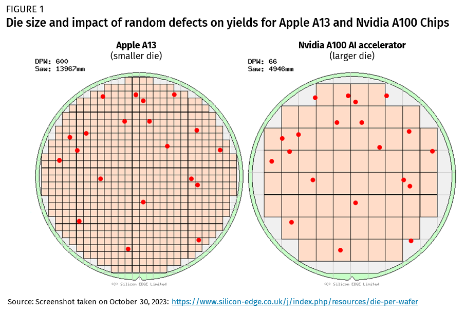
However, producing high-performance AI accelerators and server processors using DUV is much harder than producing smartphone SoCs with DUV. This is because production of AI accelerators and high-performance server chips tends to rely on larger dies (the “die” is the piece of silicon in the chip containing the integrated circuit itself). Larger dies allow more surface area to pack in more transistors (and thus computing power), but they are more complicated to produce. This is especially true for multi-patterning processes that incur a higher potential for error. In our earlier example of Apple’s A13 processor, the die area was 98.48mm², eight times smaller than Nvidia’s A100 AI accelerator, also produced on TSMC’s N7 node using DUV with a die area of 826mm².
The larger the die, the higher the stakes. Semiconductor yield is calculated by the number of functional dies per wafer produced. If 600 dies of an A13 chip fit on a 12-inch wafer, and we assume 20 random defects, this would produce 580 known good dies, or 97% yield. By contrast, only 66 dies of Nvidia’s larger A100 chip fit on a single 12-inch wafer, so 20 random defects would result in 46 known good dies, or 70% yield (see Figure 1). This example roughly illustrates why it is more costly to produce larger dies on smaller process nodes and why Chinese chipmakers will face challenges in manufacturing high-performance computing chips on older DUV equipment.
Will SMIC eventually be able to indigenously produce Biren’s AI accelerator on its 7nm DUV process? With enough resources and an acceptance of high costs and lower yield, it might. But the US controls reaching back further on DUV restrictions are designed to make that road as long and arduous as possible.
SMIC and its partners in China’s advanced packaging ecosystem like JCET are working on ways to address the limitations of its older equipment. Innovative “chiplet” designs allow manufacturers to split up the chip into smaller functional blocks that are separately manufactured to improve yield, and then combined again in the final chip through advanced packaging techniques like heterogenous integration. US controls for now appear to be more focused on front-end manufacturing inputs than back-end advanced packaging techniques, with the important caveat that exemptions apply so long as advanced packaging activities do not modify the integrated circuit’s technical performance level. The lengthy October 17 update to the original October 7 rules is a reminder of how US restrictions are likely to tighten alongside China’s advances in chipmaking, whether in advanced packaging, utilization of non-silicon materials, or photonic chips.
A growing compliance burden
With the US tightening controls to cover older-generation DUV machines, China’s ability to source spare parts and maintain the DUV machines already in its possession is in question. The BIS rules qualify that the restrictions apply to facilities involved in the “development” or “production” of “advanced-node integrated circuits” and state an intent to avoid “restricting servicing (including installation) at legacy-node facilities,” likely with an eye toward avoiding disruptions in existing electronics supply chains. But the language makes clear that the burden remains on exporters like ASML and their Chinese clients to verify that “100% of the items” are not being used for advanced node production, or else they will face licensing restrictions. With China’s chipmakers under the gun to accelerate advanced node production, parsing between advanced node and legacy chip production at foundry sites with multiple production lines could prove to be a heavy, ongoing compliance burden for foreign SME suppliers.
BIS expects technology firms to also keep abreast of China’s innovation in meeting evolving compliance standards. The new rules include “red flags” for companies to help them screen against circumvention risks. In trying to account for inevitable Chinese technological leaps, “red flag 15” in the advanced semiconductor rule describes a scenario where “a customer’s website or other marketing materials indicated that the company had advertised or otherwise indicated its capability for “developing” or “producing” “advanced-node integrated circuits.” Companies applying the new red flag screening would thus have to account for scenarios like the Huawei Mate 60 Pro Hisilicon Kirin 9000s processor in reviewing whether the advancement of Chinese firms requires fresh compliance checks for companies in the supply chain that could have enabled that progress.
Extending a long(er) arm
Among the most novel features of the original October 7 rules was the application of Section 744.6 of the EAR, which restricts the activities of US persons, to apply extraterritorial controls. This resulted in an overnight scramble for licenses by China-based fabs owned by Samsung, SK Hynix, and TSMC, and it set off months of negotiations to determine whether US regulators could trust foreign-owned fabs to keep restricted items out of the hands of Chinese chipmakers. The US persons move had a far-reaching impact, prompting companies in other industries to audit their vulnerabilities to the potential future application of US persons controls. In the new October 17 rules, BIS creates carveouts for partners that aim to mitigate the unintended consequences of the US persons rule marking US talent as liabilities for foreign firms trying to keep a foothold in the China market.
In the October 17 update, BIS put less emphasis on the US persons rule but still got creative in expanding long-arm controls beyond China (and Macau) to intermediary countries that might help China circumvent export controls. At the same time, BIS attempted to apply a more constructive tone to the rules in highlighting the benefits of being a US partner when it comes to licensing exemptions and streamlined processing for when licenses are warranted.
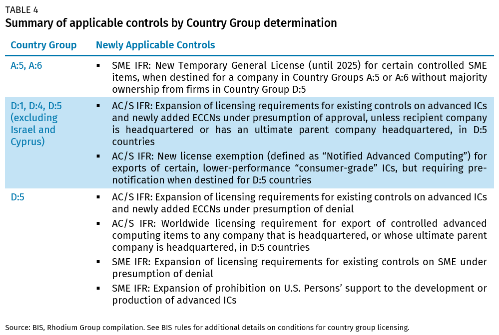
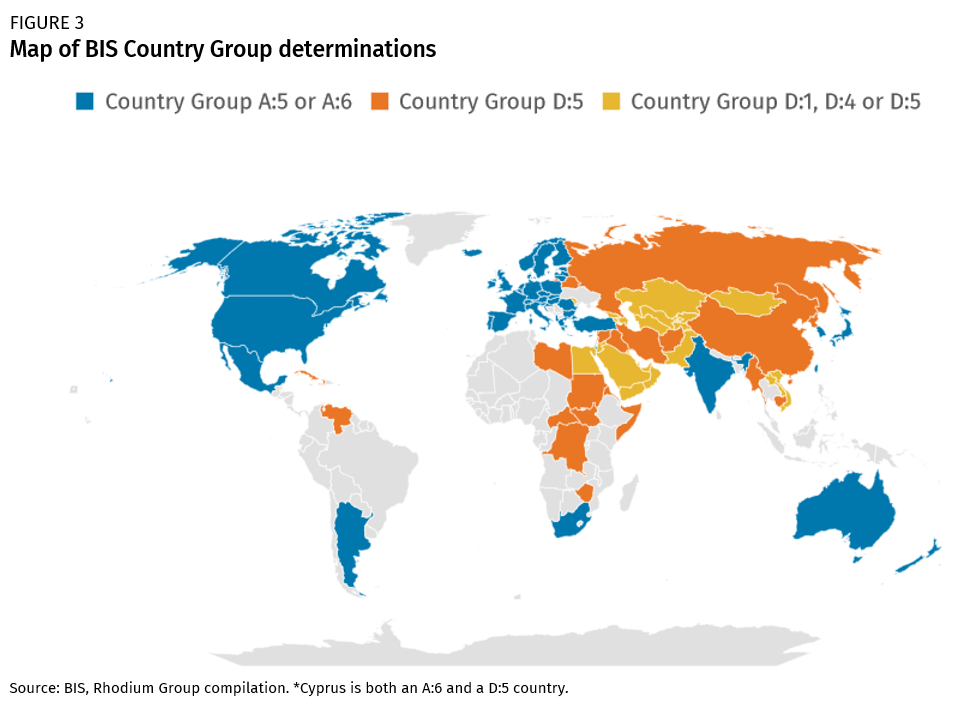
The Commerce Department determines which countries are subject to stricter or more permissive export control by categorizing them into Country Groups. In the October 17 rules, BIS imposed different restrictions on Group A countries (more trusted) versus Group D countries (less trusted) with the aim of mitigating the risk of China circumventing of export controls through third countries (see Table 4). In drawing a distinction between Commerce Group A countries for US partners eligible for licenses and exemptions and Group D countries for unreliable entities under US arms embargo or other restrictions for national security reasons, the US is effectively sketching a geopolitical map for US-China technology competition (see Figure 3).
In some cases, the new rules are given global reach to prevent export control circumvention. Restrictions can apply worldwide for cases in which the “direct product” of high-performance compute controlled items (EECN 3E001 technology for ECCN 3A090 items) is destined to an “entity headquartered in (or whose ultimate parent company is headquartered in)” a Country Group D:5 country, including China and Macau. The worldwide application is triggered any time these entities are a party to the transaction involving the foreign-produced item, including as a “purchaser,” “intermediate consignee,” “ultimate consignee,” or “end-user.”
BIS invokes this description of “entities that are headquartered in, or whose ultimate parent company is headquartered in” Macau or Country Group D:5, throughout the rules, both in qualifying partner exemptions and in specifying end-user controls. This phrasing appears designed to deter third parties from hosting or collaborating with Chinese firms to produce high-performance chips that meet the updated BIS parameters.
This “entities” provision raises serious questions on the sustainability of MNC partnerships with China-headquartered firms and their subsidiaries in developing commercial applications involving high-performance chips and related services (for instance, advanced chips used in autonomous driving that may not yet meet current parameters but that might cross that line within 3-5 years as technology advances.)
Dear partners, you’re welcome…?
The new country restrictions and exemptions are replete with nuances and caveats meant to encourage diversification away from China without upending global supply chains or overly antagonizing US partners. For example, the rules create a new Temporary General License (TGL) for US-headquartered companies and companies headquartered in Group A:5 and A:6 countries. It also makes clear that the December 31, 2025 expiry date is meant to give partners “additional time to identify alternative sources of supply.” In other words, South Korean memory chipmakers and TSMC are still on the BIS licensing hook to continue operating in China and are facing a deadline to diversify.
Finally, the 0% de minimis rule for certain lithography equipment discussed above is remarkable. This rule effectively asserts that even if no obvious US linkage exists via a person, technology, product, or service, the US nonetheless “retains jurisdiction over such foreign-made equipment to protect US national security and foreign policy interests.” To what extent US technology and security partners, such as the Netherlands, push back on the long-arm lithography restrictions remains to be seen. We see potential for the US and Netherlands to negotiate a middle ground (for example, ongoing due diligence requirements for a handful of fabs in question in China.)
The year behind and ahead
The geopolitical climate has evolved considerably since the US shook the world with the October 7 controls one year ago. Reflecting on the past year, the following themes stand out:
- Chinese retribution is on full display. From symbolic moves like Chinese legislators codifying the right to countermeasures to concrete actions like a selective product ban on US memory chipmaker Micron and export restrictions on gallium, germanium, and graphite (critical inputs for semiconductor and battery production) Beijing has been telegraphing its options to strike back at US-led chip controls and disrupt technology value chains.
- But Chinese retaliatory moves did little to temper US-led technology and investment controls. In addition to the October 17 package of rules discussed here, the US rolled out a new outbound investment screening tool in August with a broader scope for semiconductors and unanswered questions on AI (see August 11, “Big Strides in a Small Yard”). Final CHIPS Act guardrails applied stringent conditions on CHIPS Act recipients to deter future investments in China.
- The US resurrected diplomatic “guardrails” with China. US cabinet officials stepped up their outreach to China, with three secretary-level visits since June. One of these visits established an export control working group to communicate intentions and red lines on tech restrictions, though Beijing may be questioning the value of this high-level diplomatic channel given how much punch is packed into the details of the October 17 controls.
- China was able to demonstrate technological breakthroughs despite US and partner chip controls. Recent teardowns of the SMIC-manufactured Kirin 9000s SoC and YMTC-manufactured 3D NAND flash memory chip revealed the tenacity of China’s chipmakers (all while stockpiling of SME and China-compliant chips soared.)
- The US was largely able to steer partners into alignment. Japan and the Netherlands followed through with their own export controls (even as the US is now spinning up another round of negotiations with The Hague with its new long-arm lithography controls). The US was also able to bring together Japan and South Korea in a trilateral security summit where supply chain resilience for semiconductor manufacturing is a key feature of these talks (alongside parallel discussions with Taiwan.)
- The EU activated its regulatory toolkit in targeting China-made EVs with an anti-subsidies investigation, passing a new Anti-Coercion Instrument, and rolling out its new Carbon Border Adjustment Mechanism. With the EU now leaning in with measures to “level the playing field” and the US and Japan following closely behind, China faces a much bigger challenge in trying to sow divisions among G7 countries. At the same time, European nations, especially Germany will be reticent to mirror US technology restrictions while the EV probe is underway and retaliatory risks run high.
- AI innovation surges while regulators try to keep up. The past year has seen a range of regulatory actions toward generative AI, with China and Europe leaning toward a more restrictive approach, India scaling back after initially applying a heavy hand, and the US trying to find a balance between stimulating innovation and drawing boundaries with a new Executive Order on AI. The pace of technological development is catalyzing US and G7 partner discussions on AI standards and norms, how to govern cross-border data flows and define dual-use AI foundation models. This dynamic is pushing China toward a potential ‘breaking point’ in its own data security regime as it weighs the economic consequences of being excluded from emerging US and partner AI ecosystems.
Looking ahead
These geopolitical features will inform the next regulatory, diplomatic, and retributive moves to come. Our watch list for the post-October 17 world includes the following:
- Partner negotiations with a political deadline. The US-Netherlands negotiation on licensing conditions for lithography equipment will be most urgent, but the Dutch won’t be alone. Germany (whose companies like Trumpf produce machine tools and lasers, and Zeiss, which produces optics for semiconductor manufacturing) and South Korea, whose leading SME players include SEMES, Wonik IPS, PSK, and Eugene Tech, will be high on the US priority list for discussions on export control alignment. And with the November 2024 US presidential election looming, the US administration can put it to partners on whether they would rather reach an understanding with the current administration or take a gamble on the next one.
- Controls creeping into the cloud space. The October 17 controls contain a seedling of restrictions on “chips as a service” that is likely to grow bigger in time. The new rules include an end-use control on high-performance computing items to prevent companies headquartered in D:5 countries, including China, to set up cloud or data servers in other countries. The reason cited is that China could access high-performance compute capacity “to train AI models in ways that would be contrary to national security.” In its solicitation for public comment, BIS also reveals an intention to regulate infrastructure-as-a-service (IaaS) providers to restrict customers involved in dual-use AI foundation model production. This could escalate US-China tech competition to another level as Chinese cloud service providers run into compute limitations, and US cloud service providers in China face tighter restrictions from Chinese authorities in response.
- Where to draw the line on consumer-grade AI, integrated circuits, and connected systems? The October 17 rules grapple with how to distinguish between consumer and potential dual-use applications for AI and advanced computing chips in trying to determine where restrictions should kick in. For example, data center usage (plus performance threshold) is a key factor for BIS in determining which transactions involving high-performance computing chips will be restricted outright, and which now require notification. BIS is also soliciting public comment from cloud service providers on how they would monitor and flag to BIS when their customers are “developing” or “producing” a dual-use AI foundation model. Parallel to the export control buildout, outstanding questions remain over how Treasury will scope dual-use AI applications in new outbound screening rules. The BIS rules include provisions highlighting exceptions for “consumer communications devices” in the October 17 rules. BIS also notes that it has not (yet) classified network security appliances or DNA sequencing machines. That said, BIS has advised companies to screen for encryption functionalities in determining whether a technology product or service could come under restriction (the US applies the rare 0% de minimis provision for certain encryption products.) Notably, BIS also added new ‘.z’ designations to ECCNs to clarify controlled items that also meet the high-performance compute threshold. Given the fast pace in which AI-powered technologies are proliferating, BIS is trying to lay the groundwork through these rules to ensure the US list of controlled items can keep pace with potential dual-use applications.
- Minding the legacy chip conundrum. US regulators appear mindful of sticky dependencies on China for legacy chipmaking (see March 3, “Running on Ice: China’s Chipmakers in a Post-October 7 World”). Given BIS’s export control mandate, the rules focus on where the agency has drawn the line on advanced process node chips while carving out exceptions for legacy chip node production, including exemptions for servicing lithography equipment not used for advanced node production. BIS has also so far refrained from elevating controls on SMIC from its current BIS Entity Listing to Foreign Direct Product rule designation. BIS restraint is likely linked to concerns over creating bigger supply chain disruptions in electronics supply chains given China’s growing role in legacy chip manufacturing. At the same time, US policymakers have voiced concern over China growing its “coercive leverage” in commodity chips and are pointing to China’s export restrictions on critical materials as evidence of the risk. This concern will be dealt with via other regulatory tools, such as conditions on US CHIPS Act fund recipients to deter them from investing in expanding China’s semiconductor manufacturing capacity, incentives for fund recipients to reserve capacity for legacy chipmaking in the name of supply chain resilience, and potential “level the playing field” measures targeting China’s chipmakers over market distortions created by subsidies.
- The retribution factor. As noted above, China has already been demonstrating its retaliatory leverage at the lower end of electronics, chip, and battery supply chains. The question ahead is whether China’s retribution intensifies as the US proceeds apace with tech controls. Foreign technology firms are at the highest risk of becoming targets in areas where Chinese companies pose credible competition (for example, OPPO/Xiaomi/Vivo/Huawei versus Apple, Luxshare versus Foxconn, or Dell and HP versus Lenovo). US and partner-headquartered firms may face a higher risk of product bans, either informally or explicitly, on cybersecurity grounds. MNCs relying on US cloud service providers in China or Chinese cloud service providers with operations overseas may face challenges ahead as new restrictions risk setting off a chain reaction for retaliatory moves in the cloud space.
Placing a big bet
The Sullivan doctrine is alive and well in the October 17 controls. The new rules emphasize the US National Security Advisor’s “preempt and deter” posture toward protecting a US and partner tech ecosystem and the accepted ambiguity that comes with regulating fast-moving disruptive technologies. This is a paradigm shift that the corporate world is still trying to internalize with each regulatory rollout, whether in export controls, industrial policy guardrails, investment screening, trade defensive measures, or emerging data and AI governance policies.
For China, the stakes are clearly rising. Even as semiconductor manufacturing tops China’s priority list for industrial policy and tech self-reliance, China’s fiscal capacity at the local government level is highly constrained (see August 23, “The Myth of China’s Fiscal Space”). This dynamic can lead to trade-offs at the local government level between science and technology-related spending and other vital funding demands like pensions and social security, not to mention interest payments on rising local government debt. With inbound foreign investment stagnating, Beijing must make trade-offs between showcasing retaliatory leverage and sustaining China’s appeal to foreign investors. For example, even as China is restricting critical inputs to tech supply chains (and inadvertently energizing G7 de-risking policies), Chinese regulators are trying to reassure foreign investors with a partial easing of cross-border data regulations.
But China’s tech champions face an uncertain future in the wake of the October 17 controls. On the one hand, state support and retaliatory moves that cut down foreign competition can carve out more market share for domestic players. On the other hand, China faces critical vulnerabilities in semiconductor supply chains that are foundational to its economic growth. If, for example, China struggles to indigenously produce chips at scale for its data centers, Xi Jinping’s vision of “digital China” to spur new economic growth with big data infrastructure buildouts will come into question. With companies like Alibaba, Tencent, and Baidu innovating at the nexus of AI and cloud computing, will US-led dual-use controls begin to impact China’s tech champions more directly, pushing Beijing toward more aggressive forms of retaliation? And will a cornered Beijing view earnest US appeals for diplomatic and military guardrails amid this tech escalation as leverage to demonstrate the consequences of not picking up the phone when a security crisis emerges?
US National Security Advisor Jake Sullivan appears to be placing a bet that time and innovation is on the United States’ side while China’s statist approach to managing its economy will result in more fumbles than breakthroughs. As Sullivan wrote in a recent Foreign Affairs essay, “we need a sustained sense of confidence in our capacity to outcompete any country. The past two and half years have upended assumptions on the relative trajectories of the United States and China.” The October 17 controls are brimming with such confidence, all while China’s structural economic challenges have been brought into sharp relief. US faith in diplomatic guardrails to manage this escalation, however, may be premature.
This note has been prepared in collaboration with Jan-Peter Kleinhans at Stiftung Neue Verantwortung.
1. According to the new rules, total processing performance (TPP) = 2 * MacTOPS * bit length of the operation (aggregated processing units on the integrated circuit). “Mac” stands for “multiply-accumulate computation” (D = A × B + C) and BIS states that “2 * MacTOPS may correspond to the reported TOPS or FLOPS on a datasheet.” The intent is to capture the theoretical peak number of Tera operations per second for multiply-accumulate computation.
2. The EAR defines “advanced-node” integrated circuit to include ICs that meet any of the following criteria: (1) logic ICs using a non-planar transistor architecture or with a “production” technology node of 16/14 nanometers or less; (2) NOT AND (NAND) memory ICs with 128 layers or more; or (3) dynamic random-access memory (DRAM) ICs using a “production” technology node of 18 nanometer half-pitch or less